Nanotechnology creates great application opportunities

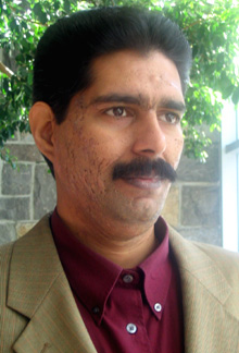
Sivakumar Narayanswamy
Photo by Xamia Keane
The niche that engineer Sivakumar Narayanswamy has created for himself is a very small one, but it has huge potential.
His work focuses on nanotechnology, a nanometer being one billionth of a meter, or about 1/100,000 the width of a human hair.
“Nanotechnology is the new buzzword in the industry,” said Narayanswamy, referring to fields such as microelectronics and biotechnology. “This is relatively an uncharted area, so there is scope for about 30 or 40 years of work to be done.”
Narayanswamy arrived at Concordia’s Department of Mechanical and Industrial Engineering about six months ago to fill a new Canada Research Chair in Laser Metrology and Laser Micromachining.
This Tier 2 chair for exceptional emerging researchers brings a total of $500,000 to the university over five years. Narayanswamy plans to use it to set up a laboratory for laser metrology and micromachining in the new engineering building.
Narayanswamy was born in Chennai, in southern India, and did his undergraduate degree at Madras University and a Master’s in Engineering Management at Queensland University of Technology in Australia.
He then went to Singapore in 1997 to begin a PhD program at Nanyang Technological University, just as that institution was setting up a strategic research program to complement Singapore’s hard disk drive, semiconductor, and microelectronics manufacturing industries. There he developed an expertise in interferometry, a technique that uses a split laser beam to measure with accuracy in the range of nanometers.
There are several applications for such high precision measurements and he gives the example of hard disk drives. Hard disks can hold vast amounts of information, so a sensor (slider), sitting just above the rotating disk, must be able to distinguish between and read very densely packed lines.
“The gap between the slider and the hard disk may be 10 to 15 nanometers at this stage, and is expected to go to five to seven nanometers in the future. We need to control these distances very accurately, so we need a very precise measurement system,” he explained.
Vibrations in the spinning disk have to be taken into account, and surface smoothness is another crucial factor. When you are this close, you don’t want the surface to be rough.
“This is the equivalent of flying a 747 airplane within 1.5 millimeters of the runway,” so even small variations in the surface are unacceptable. He is using interferometry to measure these variations, and is also applying interferometry to micromachining.
Using the method he has developed, low-power lasers can efficiently measure small defects, both on the surface and on the sub-surface. “We can use this kind of machining method to suit the semiconductor, and photonics [fibre optics] industries,” he explained.
Narayanswamy’s work also has applications in microelectronics. These devices are not only shrinking in size, they have more functions, so components are being packed closer together. “If you are going to put transistors so close together, you have to be able to measure the distances between them.”
Narayanswamy will collaborate with Concordia’s team of MEMS researchers. MEMS (micro-electro-mechanical systems) are devices that are micrometers in size and have a variety of applications, such as pressure sensors for vehicles, heat sensors for aerospace applications, and as drug delivery systems.
His research will not only put Concordia on the leading edge of this expanding field, it will have immediate applications in Canadian industry, leading to savings in time and cost, and increasing the value of end products.